
GeForce 9500 GS
Key Metrics
- Launch Date
- 2008-07-29
- CUDA Cores
- 32
- Memory
- 512 MB DDR2
- Memory Bandwidth
- 16.13 GB/s
- TDP/TBP
- 40 W
- Interface
- PCIe 2.0 x16
Add to comparison
Save this GPU, then open another GPU page to compare them side by side.
Or compare with:
GPU Gallery
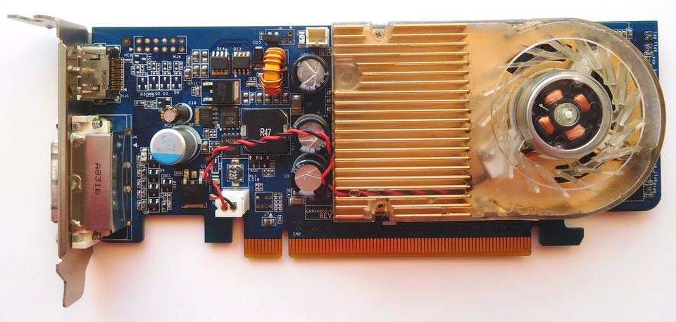

Why It Mattered
GeForce 9500 GS belongs to the Tesla and GeForce 9 Series era around 2008, when PC graphics cards varied heavily by bus, memory chips, BIOS, cooler, and display outputs. Tracking the exact model helps retro builders distinguish period-correct boards from similarly named variants.
Sources
Independent reference sources
- TechPowerUp GPU SpecsModel-level specification reference for this GPU entryOpen source
Reference databases
- RightNow GPU DatabaseOpen GPU database used to cross-check specifications A reference database: good for cross-checking specifications, but not proof of the original release details on its own.Open source
Photo sources
- Wikimedia CommonsPhoto: GeForce 9500 GS 512 MB DDR2 PCIe board (Front)Creator: Cjp24Credit: Cjp24 / Wikimedia CommonsTitle: Nvidia GeForce 9500 GS, 512MB (1)License: CC BY-SA 4.0 InternationalSource claim: Commons credits Cjp24 and states CC BY-SA 4.0 International for this exact file.Modified: Resized to 960 px maximum dimension and JPEG recompressed; no crop. This derivative is shared under CC BY-SA 4.0 International.Board identity: The photographed example is identified on its exact Commons file page.Configuration: The source identifies 512 MB DDR2, matching the Wiki memory fields; the photograph does not establish PCIe transfer generation or clocks.License deedOriginal file page