
GeForce 6800 Ultra
Key Metrics
- Launch Date
- 2004-07-26
- Memory
- 256 MB GDDR3
- Memory Bandwidth
- 35.2 GB/s
- TDP/TBP
- 81 W
- Interface
- PCIe 1.0 x16
- Process Node
- TSMC 130 nm
Add to comparison
Save this GPU, then open another GPU page to compare them side by side.
Or compare with:
GPU Gallery

Sources
Primary / manufacturer sources
- Montrym and Moreton, The GeForce 6800, ACM Queue PDF mirrorArchitecture source authored by NVIDIA engineers.Open source
- HotHardware, NVIDIA GeForce 6800 reviewPeriod review context for NV40-derived GeForce 6800 family positioning.Open source
- NVIDIA Linux README supported products, Release 100.14.23Official driver support list context for legacy GeForce products.Open source
- NVIDIA GeForce 6 Series Product OverviewOfficial NVIDIA comparison identifying a 256-bit effective memory interface for GeForce 6800 models across AGP and PCI ExpressOpen source
Independent reference sources
- TechPowerUp GPU SpecsModel-level specification reference for this GPU entryOpen source
Reference databases
- RightNow GPU DatabaseOpen GPU database used to cross-check specifications A reference database: good for cross-checking specifications, but not proof of the original release details on its own.Open source
Photo sources
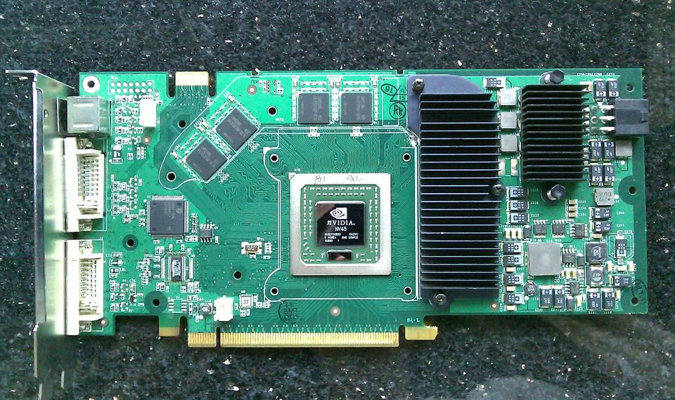
- Wikimedia CommonsPhoto: NVIDIA GeForce 6800 Ultra 512 MB engineering-sample PCIe board (Front)Creator: HyinsCredit: Hyins / Wikimedia CommonsTitle: NVIDIA GeForce 6800 Ultra 512MBLicense: Public domain creator dedicationSource claim: Commons creator Hyins dedicates this own-work GeForce 6800 Ultra 512 MB engineering-sample photograph to the public domain.Modified: Resized to 960 px maximum dimension and JPEG recompressed at quality 78; no crop.Board identity: The exact photographed example is identified on its Commons file page.Configuration: The source states 512 MB while the Wiki reference lists 256 MB GDDR3. The photograph does not establish memory type or PCIe signaling generation.Original file page