
EGA Wonder 800+
Key Metrics
- Launch Date
- 1988-01-01
- Memory
- 262 KB DRAM
- Memory Bandwidth
- 0.032 GB/s
- Interface
- ISA 8-bit
- Process Node
- NEC 800 nm
- Bus Width
- 32-bit
Add to comparison
Save this GPU, then open another GPU page to compare them side by side.
Or compare with:
GPU Gallery

Sources
Independent reference sources
- TechPowerUp GPU SpecsOpen source
Photo sources
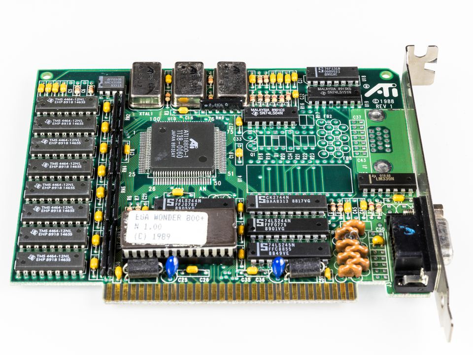
- Wikimedia CommonsPhoto: ATI EGA Wonder 800+ ISA board (Front)Creator: Raimond SpekkingCredit: Raimond Spekking / Wikimedia CommonsTitle: ATI EGA Wonder 800+-9838License: CC BY-SA 4.0 InternationalSource claim: Commons credits Raimond Spekking for this own-work Wonder 800+ board photograph and publishes it under CC BY-SA 4.0.Modified: Resized to 960 px maximum dimension and JPEG recompressed at quality 78; no crop. This derivative is shared under CC BY-SA 4.0 International.Board identity: The exact photographed example is identified on its Commons file page.Configuration: The pictured board has a 1989 ROM label while the Wiki release year is 1988. The image does not prove the Wiki 262 KB DRAM capacity or ISA operating mode.License deedOriginal file page