
Radeon R9 Nano
Key Metrics
- Launch Date
- 2015-08-27
- Stream Processors
- 4,096
- Memory
- 4 GB HBM
- Memory Bandwidth
- 512 GB/s
- TDP/TBP
- 175 W
- Interface
- PCIe 3.0 x16
Add to comparison
Save this GPU, then open another GPU page to compare them side by side.
Or compare with:
GPU Gallery

Sources
Independent reference sources
- TechPowerUp GPU SpecsOpen source
Photo sources
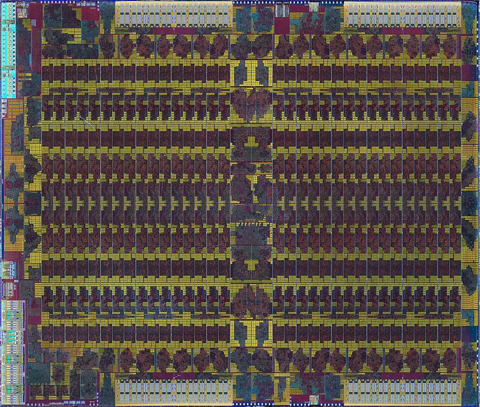
- Wikimedia CommonsPhoto: Radeon R9 Nano Fiji chip photograph (Die view)Creator: Fritzchens FritzCredit: Fritzchens Fritz / Wikimedia CommonsTitle: AMD@28nm@GCN 3th gen@Fiji@Radeon R9 Nano@SPMRC REA0356A-1539 215-0862120 DSCx1 polysilicon@5x.jpgLicense: Public domain under CC0 1.0 UniversalSource claim: Commons credits Fritzchens Fritz and states the creator dedicated this exact image to the public domain under CC0 1.0 Universal.Modified: Resized from the source-supplied 960 px Wikimedia rendering and JPEG recompressed; no local crop. Public domain under CC0 1.0 Universal terms retained.Board identity: The exact Commons file page identifies this photographed example.Configuration: This Fiji die view illustrates the source-identified Radeon R9 Nano chip. It does not establish board maker, memory configuration or reference clocks. The creator identifies a sanded polysilicon-layer microscope view.License deedOriginal file page