
Radeon RX Vega 56
Reference GPU
GCN 5.02017
3,584 Stream Processors · 8 GB HBM2 · 210 W
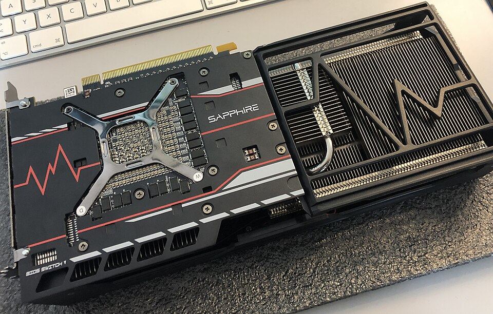
GPU Wiki Architecture
GCN 5.0 (Vega) launched in 2017 with a focus on compute density and high-bandwidth HBM2 memory. The Radeon RX Vega 64 and Vega 56 were the consumer flagships, built on the large Vega 10 die at 14nm.
Vega offered strong FP16 and FP64 compute throughput and substantial HBM2 frame buffers, making it popular for GPU compute workloads and cryptocurrency mining, though it consumed more power than competing NVIDIA Pascal products at similar performance levels.
HBM2 memory: up to 8 GB at 484 GB/s on Vega 10, providing substantially more bandwidth than GDDR5X competitors.
Rapid Packed Math: FP16 operations at 2x the rate of FP32, enabling faster compute on half-precision workloads.
Next Compute Units (NCUs): redesigned Compute Units with improved instruction cache and prefetch.
High Compute Unit count (64 CUs on Vega 10) targeting professional and compute-oriented workloads.
Vulkan 1.1 compliance.
Vega occupied AMD's high end at a time when GCN was approaching architectural maturity on 14nm. Its HBM2 integration and compute focus made it a preferred platform for early machine learning researchers who needed AMD hardware, and its large frame buffers made it useful for professional visualization. The generation's higher power draw relative to Pascal was a recognized weakness, and it accelerated AMD's development of the cleaner RDNA architecture.