
Quadro NVS 285
Key Metrics
- Launch Date
- 2006-06-06
- Memory
- 128 MB DDR2
- Memory Bandwidth
- 4.8 GB/s
- TDP/TBP
- 18 W
- Interface
- PCIe 1.0 x16
- Process Node
- TSMC 110 nm
Add to comparison
Save this GPU, then open another GPU page to compare them side by side.
Or compare with:
GPU Gallery
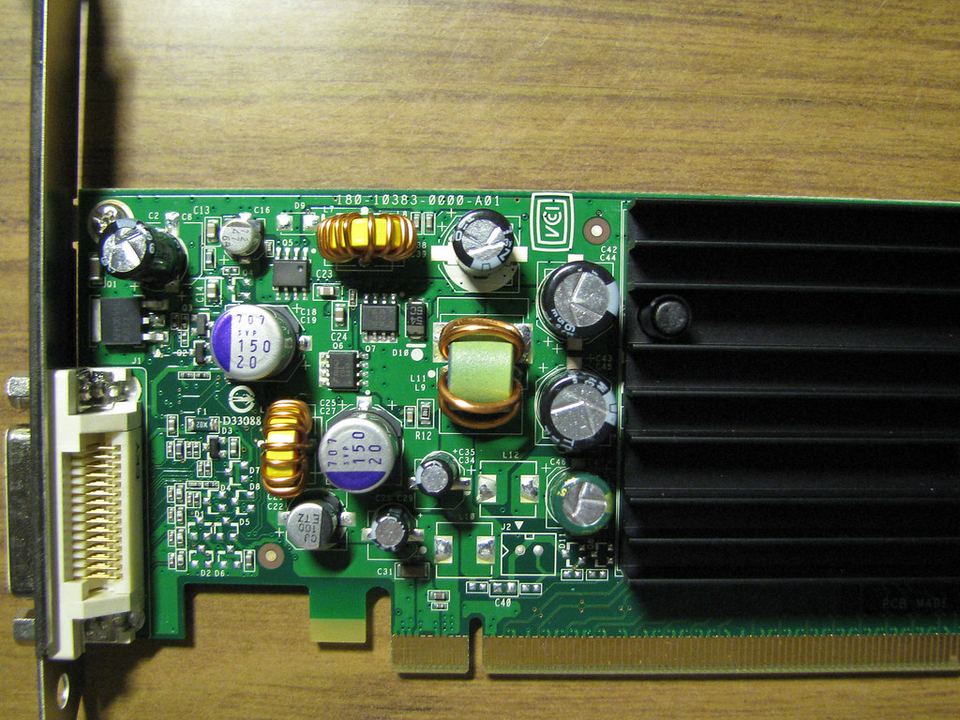
Why It Mattered
Quadro NVS 285 sits in NVIDIA's business-display and NVS lineage, where multi-monitor stability, small form factors, and enterprise driver support mattered more than gaming performance. Exact board details are important because NVS cards often changed outputs, brackets, and OEM packaging.
Sources
Independent reference sources
- TechPowerUp GPU SpecsModel-level specification reference for this GPU entryOpen source
Reference databases
- RightNow GPU DatabaseOpen GPU database used to cross-check specifications A reference database: good for cross-checking specifications, but not proof of the original release details on its own.Open source
Photo sources
- FlickrPhoto: NVIDIA Quadro NVS 285 PCI Express board (Front)Creator: Edmund TseCredit: Edmund Tse / FlickrTitle: Nvidia Quadro NVS 285License: CC BY 2.0 GenericSource claim: Flickr credits Edmund Tse and marks this exact photograph CC BY 2.0.Modified: Resized to 960 px maximum dimension and JPEG recompressed; no crop. CC BY 2.0 attribution retained.Board identity: The photographer identifies this physical board on the exact Flickr photo page.Configuration: The photo does not establish the Wiki entry’s 128 MB DDR2 memory or PCIe signaling generation.License deedOriginal photo page